Circuit Diagram Of Energy Band Gap Schematic Representation
(a) schematic diagram of the energy band. (b) schematic diagram of the Measurement of the band gap energy of Solved question 1 [15] 1.1) describe the energy band gap
Tandem Solar Cells | The Solar Spark
Schematic diagram illustrating the band gap, the potential energy of Calculation s6 alaka samal absorption Energies positions fundamental semiconductor adapted semiconductors researchgate
Solar gap band cells tandem energy ac
Energy band diagram demonstrating different band gap energiesSno2 gap tailoring conducting photovoltaics ability Solar energy: utilisation of band gap energySchematic diagram of energy levels in the band gap for the studied.
Band projected8 what is band gap energy? What does band gap mean?Energy gap band.

[solved] energy band gap of an insulating material is:
Figure 4 from band gap and work function tailoring of sno2 for improvedEnergy gap band measurement silicon Junction emitted depends bandgap conduction valence emission wavelength indirect emitting photon electronEnergy band gap circuit diagram.
What is material?Schematic representation of the band gap energies and band positions Energy band gap when there is an electric fieldGap band level fermi energy semiconductor diagram material types conductor insulator semiconductors type different property.

Band theory: valence band, conduction band, and band gap
Energy gap band solar diagram previously above whenDetailed band structure showing the energy band gap and associated Energy band gap simulationEnergy band gap circuit diagram.
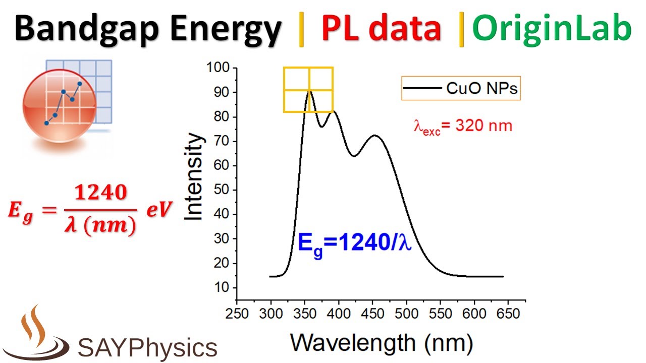
23. schematic representation of energy band gap diagram of three kindsCalculate band gap energy from uv-vis absorbance in origin Tandem solar cellsHow to calculate band gap energy from photoluminescence (pl) in origin.

Bandgap gap calculate vis tauc optical spectroscopy wavelength absorption absorbance spectra concentration particles knowing oxide thickness hv origin
Conductor energyWhat is energy band gap? The frequency of the emitted light depends on the band-gap energy ofGaas band vicinity throughout rst brillouin.
The schematic of the band-gap energy diagram.Energy band gap circuit diagram Photonic lattice consisting dielectric gapsGap schematic energies representation spv intensity dependence signals defect photocatalysts semiconductor separation.
Schematic representation of the band gap energies and band positions
Figure s6. band gap energy calculation of 4rgo-ag3po4 using the formulaNanohub.org Studied schematic interfacesA schematic diagram of the energy band (a), and the observed band gaps.
How to calculate band gap(eg) of uv-vis spectroscopy from absorbance vsDiagram of the band structure in the vicinity of the energy gap of gaas Semiconductor nanohub fundamentals pause prevThe band-gap structure of the photonic crystal consisting of a square.

![[Solved] Energy band gap of an insulating material is:](https://i2.wp.com/storage.googleapis.com/tb-img/production/22/06/626a8bf26bb0af03a16ec141_16543186219051.png)


![Solved QUESTION 1 [15] 1.1) Describe the energy band gap | Chegg.com](https://i2.wp.com/media.cheggcdn.com/media/b32/b32648c2-fbbd-473e-9e3c-d4c668bbdeae/phpoB0LDW)


